Al2O3 Enabling High-Tech Applications with Precision and Reliability

Advanced Aluminum Oxide (Al2O3): Enabling High-Tech Applications with Precision and Reliability


Abstract


Aluminum oxide(Al2O3), commonly known as alumina, is a versatile and high-performance ceramic material widely utilized across numerous advanced industries due to its exceptional dielectric strength, thermal stability, chemical inertness, and mechanical hardness. This paper outlines the key properties, applications, and technical specifications of high-purity alumina, with a focus on its critical role in semiconductor packaging and lithium-ion battery coatings. Additionally, it highlights the manufacturing and supply capabilities of UrbanMines Tech., a leading Chinese producer committed to quality, customization, and reliable export services.


1. Introduction


Alumina is not merely a raw material for aluminum production; it is a cornerstone of modern high-technology manufacturing. From microelectronics and energy storage to optics, catalysis, and protective coatings, alumina’s unique combination of properties makes it indispensable. With the growing demand for miniaturization, energy efficiency, and high reliability in electronic and energy systems, the need for precisely engineered high-purity alumina has never been greater.


2. Material Properties and Specifications


High-purity alumina is categorized by its phase, purity level, particle size distribution, and trace impurity content, each parameter tailored to specific application requirements.


2.1 Purity and Impurity Control

- High-Purity Grades: 4N (99.99%), 5N (99.999%), and 6N (99.9999%) alumina are essential for sensitive applications such as semiconductor encapsulation and optical components.

- Low Alpha-Ray Emission: Critical for semiconductor packaging to prevent soft errors in memory devices. Specifications often require Uranium (U) and Thorium (Th) content below 3 ppb, with minimal Fe, Na, and Cl impurities.

- Example Specification:

  - Al₂O₃ content: ≥ 99.7%

  - SiO₂: < 0.15%, Fe₂O₃: < 0.1%, Na₂O: < 0.1%

  - Moisture: < 0.1%, Loss on ignition: < 0.1%


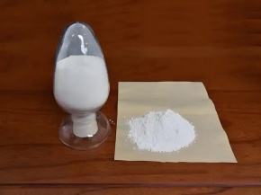
2.2 Particle Size and Morphology

Applications dictate precise granulometry:

- Spherical Alumina: D50 sizes ranging from 1 µm to 45 µm (e.g., 2.8 µm, 5.8 µm for optimized packing density in semiconductors).

- Non-Spherical Alumina: D50 from 1.5–10.5 µm, used in coatings and composites where specific surface area and green density are crucial.

- BET Surface Area: Typically < 1.5 m²/g for coatings to ensure proper slurry formulation and adhesion.


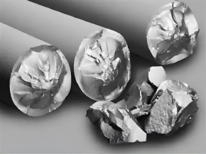
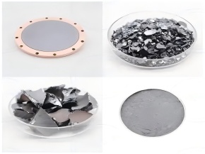
2.3 Phase and Crystalline Structure

Alpha-phase alumina (α-Al2O3) is the most thermodynamically stable form, offering superior hardness, thermal conductivity, and electrical insulation. Crystal sizes of 2–3 µm are often specified for consistent sintering behavior and final microstructure.

  • #
  • #
  • #


3. Key Applications in High-Tech Industries


3.1 Semiconductor Packaging

Low-alpha spherical alumina is used as a filler in epoxy molding compounds (EMCs) to enhance thermal conductivity, reduce coefficient of thermal expansion (CTE), and provide radiation shielding. Particle size distribution (e.g., bimodal 2.8 µm and 5.8 µm) is optimized for maximum packing and minimal viscosity.


3.2 Lithium-Ion Battery Separator Coatings

High-purity α-alumina (D50 < 4 µm) is applied as a ceramic coating on polymer separators. It improves thermal stability, prevents dendrite penetration, and enhances electrolyte wettability, thereby increasing battery safety and cycle life. The material is mixed with binders to form a stable slurry for uniform coating.


3.3 Other Advanced Uses

- Capacitors: As a dielectric barrier due to its wide band gap.

- Catalysis & Adsorption: High-surface-area alumina as catalyst support or desiccant.

- Structural Ceramics: In wear-resistant coatings, biomedical implants (e.g., hip replacements), and armor systems.

- Polishing & Abrasives: Ultrafine alumina (Diamantine) for precision polishing in optics and watchmaking.

- High-Temperature Insulation: As refractory linings in furnaces.


4. UrbanMines Tech.: A Reliable Partner from China


As global demand for specialty alumina grows, UrbanMines Tech. stands out as a trusted supplier with deep technical expertise and a customer-focused approach.


4.1 Manufacturing Excellence

- Our dedicated production lines in inland China are equipped to produce high-purity, low-alpha alumina with strict quality control.

- We offer flexible batch sizes—from R&D samples to full-scale production—ensuring short lead times and just-in-time supply.


4.2 Customization Capability

- We tailor purity, particle size distribution, morphology (spherical/non-spherical), and impurity profiles to meet exact customer requirements.

- Technical support is provided to assist with material selection and integration.


4.3 Proven Reliability and Export Expertise

- With 16 years of industry experience, we have built long-term relationships; over 60% of our clients have been partners for more than 5 years.

- We hold all necessary export licenses, including those for rare earth-related products, ensuring smooth and compliant international logistics.


4.4 The Advantage of “Made in China”

- China’s mature industrial ecosystem offers competitive advantages in raw material sourcing, advanced processing technologies, and scalable production.

- UrbanMines Tech. leverages these strengths while adhering to international quality standards (ISO, RoHS, REACH).


5. Conclusion


High-purity aluminum oxide is a critical enabler of innovation in electronics, energy storage, and advanced ceramics. Meeting the stringent requirements of modern applications demands not only advanced material science but also a reliable and agile supply chain. UrbanMines Tech. combines high-performance product offerings with responsive customization and dependable export services, making it an ideal partner for global clients seeking quality alumina solutions.


Top

When Color Meets Eternity Is the Rise of Colored Marble Disrupting Traditional Color Aesthetics?

Marble, a timeless classic, has never faded from the world of design and architecture. The combination of black and white marble, with its clean lines, has long created spaces that are comfortable, natural, and sophisticated. Yet, a new trend is quietly emerging—Colored Marble Stone—infusing spaces with unprecedented vibrancy and emotional depth through its bright, saturated tones. This leads us to wonder: is it reshaping our traditional color aesthetics?

From eternal tranquility to contemporary boldness, colored marble does not replace the classic but expands the expressive boundaries of stone. It liberates spaces from the dialogue of neutral tones, granting them a richer emotional language.

Colored Marble Application Cases: Integrating Natural Beauty into Life

1. A Staircase of Hues: In a collaborative work by architect Alan Shulman and designer Frank de Biasi, a marble staircase becomes the focal point. Its treads are clad in panels of various brightly colored stones, including vibrant Colored Marble Stone, resembling a solidified rainbow that connects not only different spaces but also tradition and innovation.


colorful marble staircase

2. An Artistic Focus in the Kitchen: In a New York apartment, designers from LeWhit eschewed a conventional backsplash in favor of gray breccia Capraia marble with burgundy speckles. This distinctive Colored Marble Stone wall instantly elevates the kitchen into a large-scale art piece, showcasing the dramatic appeal of natural stone veining.


marble backsplash

3. A Colorful Manifesto in Milan: At Milan Design Week, the collaborative project between SolidNature and OMA design studio served as a grand celebration of colored marble's beauty. Particularly noteworthy was a series of marble furniture pieces designed by architects Ellen van Loon and Giulio Margheri. Even more stunning was an installation featuring nine different types of Colored ONYX Marble, their gentle glow resembling a gateway to a natural wonderland or another dimension, highlighting the stone's innate spirituality.


colorful onyx stone

colorful onyx stone

colorful onyx stone


4.A Gravity-Defying Cabinet: A cleverly designed marble cabinet perfectly illustrates the balance between function and art. Constructed primarily from green marble with Colored Marble Stone shelves, this Marble Wall Cabinet rests on a rotating pivot. Its substantial upper mass appears to "float" precariously yet precisely on a minimal base, challenging visual perception while remaining fully functional. Designer Sabine Marcelis explored the "delicate balance between aesthetics, material, form language, and function" through this piece.


marble cabinet

marble cabinet

Behind the Trend: A Deep Longing for Nature and Permanence

Since the pandemic, there has been a profound yearning to reconnect with nature. This trend manifests in design as a shift: designers no longer merely adjust natural materials to fit a chosen concept or style. Instead, they use these materials as the core inspiration, building entire spatial narratives around them. Colored marble is the perfect vessel for this philosophy.

Designers and their clients cherish marble not only for its visual beauty but for the sense of permanence it carries—a connection to the deep history of the earth itself. It transcends fleeting trends, embodying true, lasting durability. Whether laying down a stunning Colored Marble Floor or crafting a unique feature wall with Colored Jade Marble, it reminds us that the most moving designs often stem from the unadulterated splendor and power of nature itself.

The rise of colored marble is not a disruption, but a renewal. It invites us to rediscover the infinite possibilities of natural materials with a more open and perceptive eye, allowing the classic to stride into the next eternity, blossoming with color.

Finally, let me recommend some of the stone materials :

Verde Ming Green Pink onyx Arabescato Orobico Rosso Red Light
Verde Ming Green Marble Pink onyx Arabescato Orobico Rosso Red Light Marble


ROSA NORVEGIA Marble Cold Emerald Marble Cloudy Wave Marble


Top

Using Stone Sinks When Designing a Bathroom

Stone basins prove great in unique bathroom design

When designing a bathroom there are a few things we need to consider. First of all, you should decide between modern and classic interior design. Having done that, it’s time to think about overall image of bathroom interior. For those of you after luxurious, natural and unique look of the bathroom, RF offers a great range of stone sinks, stone basins, stone baths and stone tiles, altogether creating a complete solution for bathroom design.

marble basin bathroom

Why choose stone sinks over ceramic sinks?

That’s a question some of you are going to ask anyways, so let’s focus on that for now. Some say stone basins are very expensive and intended for rich people with too much money to throw around. Well they couldn’t be more wrong! Truth is, stone sinks are practically priced the same as good quality ceramic sinks, with the advantage of being more durable and original. The very reason behind choosing a wash basin made of natural stone over a ceramic one is their uniqueness. They are in most cases one of the kind, as they are made from natural material as found in mother nature, a piece of rock given shape. Additionally, they are number one choice if you are looking for something to make your bathroom really stand out, that is look different than traditional bathrooms with white ceramic sinks and ceramic tiles seen everywhere. If you truly want your bathroom to be original, stone tiles, pebble tiles and stone sinks are your best bet.

Will stone sinks fit into any bathroom design?

The beauty of natural stone is that it fits in any design, be it classic or modern. Stone sinks and stone tiles, as well as marble tiles and pebble tiles will fit perfectly into any existing bathroom regardless of its design. But to bring out the real beauty of them the bathroom could be designed from scratch including stone tiles or pebble tiles on walls and floor as well as stone sink and maybe a touch of wood here and there. It has proved to be great mix on numerous occasions and all of our clients are extremely happy with their luxurious bathrooms, each of which is one of a kind.

marble stone sinks

Top

Why Onyx Candle Jar is Popular for Home Decor

The popularity of the Onyx candle jar in home decor is a perfect blend of aesthetic appeal, perceived wellness benefits, and timeless style. It's more than just a candle holder; it's a decorative statement piece.

Here’s a detailed breakdown of why it's so popular:

1. Striking Visual Aesthetics

This is the primary reason for its popularity. Onyx stone has a unique and captivating appearance that instantly elevates a space.

  • The Glow of Translucence: The magic of onyx is its semi-translucent quality. When a candle is lit inside, the entire jar glows with a warm, ambient, and almost magical light. The light dances through the natural veins and layers of the stone, creating a dynamic and organic lighting effect that a regular glass jar can't replicate.

  • Natural and Organic Texture: In an era where biophilic design (connecting with nature indoors) is a major trend, onyx brings a piece of the natural world inside. Each piece is completely unique, with its own patterns, veins, and color variations, from deep black to honey gold and green.

  • Luxurious and Sculptural: An onyx jar has a substantial, carved feel. It looks like a beautiful art object or sculpture even when the candle isn't lit. It adds a touch of organic sophistication and luxury to any shelf, mantel, or bathroom counter.

white onyx candle jar

2. Versatility in Style

Onyx is surprisingly versatile and can complement a wide range of interior design styles.

  • Modern & Minimalist: Its clean lines and natural material work perfectly in a minimalist setting, acting as a stunning focal point without clutter.

  • Bohemian & Global: The raw, earthy feel of onyx fits right in with boho-chic and globally-inspired decor, adding to a collected, well-traveled vibe.

  • Traditional & Glam: The stone has been used in palaces and luxury hotels for centuries. A polished onyx jar brings an old-world, opulent feel to traditional or Hollywood Regency-style spaces.

  • Industrial: The contrast between the raw, natural stone and industrial elements like metal and concrete creates a beautifully balanced and textured look.

green onyx candle jar

3. Perceived Wellness and Ambiance

The type of light an onyx jar emits is key to its appeal for creating a specific mood.

  • Soft, Ambient Lighting: The stone diffuses the candlelight, transforming a sharp flame into a soft, warm, and soothing glow. This is ideal for creating a calming, intimate, and relaxing atmosphere—perfect for unwinding after a long day, a romantic dinner, or a relaxing bath.

  • Connection to Crystal Healing: While not scientifically proven, onyx is a popular stone in crystal lore. It is often associated with properties like protection, grounding, and strength. For those who believe in or appreciate these concepts, having an onyx piece in the home adds an extra layer of intentionality and positive energy to their space.

customized candle jar with lid

4. Tactile and Quality Feel

Onyx stone is cool and smooth to the touch, giving it a heavy, high-quality, and substantial feel. This perceived quality is important in home decor, as people are increasingly investing in pieces that feel special and well-made, rather than disposable.

5. The "Instagrammable" Factor

The photogenic quality of a glowing onyx jar cannot be understated. It creates a beautiful, warm, and aesthetically pleasing scene that is highly sought after for social media platforms like Instagram and Pinterest. This exposure has fueled its trendiness and desirability.

luxury onyx canlde jar for home decor

In Summary:

An Onyx candle jar is popular because it successfully combines multiple desirable qualities:

  • It's a beautiful art piece when unlit.

  • It's a unique, organic light source when lit.

  • It fits into countless decor styles, from modern to boho.

  • It creates a specific, calming ambiance perfect for relaxation.

  • It feels luxurious, high-quality, and intentional.

It’s a simple yet powerful decorative object that satisfies the modern desire for natural materials, wellness-focused living, and instagrammable style.

Top

6N Boron in Semiconductors and Advanced Fields

Boron: From Basic Material to High-Tech Core - Analyzing the Precision Application of High-Purity Boron in Semiconductors and Advanced Fields


In high-tech fields that pursue microscopic limits and pinnacle performance, certain fundamental elements play a crucial role. Boron, element symbol B, atomic number 5, is one such element. This metalloid, found only in compounds in nature, has become an indispensable "key element" in fields such as semiconductors, advanced materials, and the nuclear industry due to its unique electronic structure and physical and chemical properties.


1. "Master Craftsmen" of the Semiconductor Industry: Precision Doping and Crystal Growth


In the semiconductor industry, the value of high-purity crystalline boron lies in its unparalleled precision control capabilities.


The cornerstone of P-type doping: Boron's core use is as a P-type dopant. Silicon (Si) is the undisputed workhorse of semiconductor materials, but inherently it conducts poorly. When boron atoms are precisely introduced into the silicon lattice through techniques such as ion implantation or high-temperature diffusion, boron's outermost shell contains only three electrons, compared to silicon's four electrons. This creates a "hole" that can accommodate and carry electrons, effectively creating a P-type semiconductor. This "doping" process is fundamental to the construction of the PN junction—the fundamental building block of all semiconductor devices, including diodes, transistors, and thyristors.


The key to power devices and scaling: In power devices that must withstand high voltages and high currents (such as IGBTs and power MOSFETs), boron-doped silicon wafers (typically in the high-resistance region) effectively regulate the electric field distribution and enhance the device's withstand voltage. Furthermore, at advanced process nodes, the formation of ultra-shallow junctions requires extremely high doping precision. Boron, due to its small atomic radius, enables finer doping control, meeting the demands of nanoscale devices.


Source material for single crystal growth: In addition to doping, crystalline boron is also used as a source material for growing boron-doped silicon single crystals via the melt process. This method produces silicon ingots with uniform P-type conductivity across the entire wafer, providing the foundation for the large-scale manufacturing of highly consistent semiconductor devices.


2. Beyond Semiconductors: Boron's Outstanding Performance in Multiple Fields


Boron's uses go far beyond semiconductors; its compounds and isotopes shine in many advanced fields.


Advanced Structural Materials: Boron's extremely high hardness (Mohs hardness 9.5) makes it an ideal material for reinforcement. Boron fibers and boride ceramics are key components in the manufacture of high-strength, lightweight composite materials, widely used in aerospace, high-performance sports equipment, and other fields.


Specialty Glass and Ceramics: In glass manufacturing, the addition of boron oxide significantly reduces the coefficient of thermal expansion, imparting excellent thermal shock resistance. This borosilicate glass is a preferred choice for laboratoryware (such as heat-resistant beakers) and high-end cookware. Similarly, the addition of boron compounds to ceramics improves their thermal stability and mechanical strength.


Neutron capture and the nuclear industry: Natural boron contains approximately 20% of the boron-10 isotope, which has an extremely high capture cross section for thermal neutrons. This property makes boron-10 (usually in the form of boron carbide or boric acid) an indispensable control rod material, neutron shielding material, and safety agent for emergency shutdown systems in nuclear reactors.


Organic Synthesis and Pharmaceuticals: In the fine chemical and pharmaceutical fields, boron-containing reagents (such as boronic acids and boronic esters) are important intermediates for building carbon-carbon and carbon-heteroatom bonds, particularly in Suzuki-Miyaura coupling reactions. An increasing number of boron-containing organic molecules are being developed as new pharmaceuticals. For example, certain proteasome inhibitors have become important anti-cancer therapies.

  • #
  • #
  • #


3. Quality is the cornerstone of technology: reliable supply from China


Faced with such extensive and demanding high-tech applications, the requirements for the purity, consistency and specific form (such as particle size and crystal form) of boron materials have reached unprecedented levels.


UrbanMines Tech., a leading manufacturer and supplier of high-purity boron materials in China , deeply understands the crucial impact of material properties on downstream products. Leveraging our proprietary and controlled production lines, we specialize in providing semiconductor-grade high-purity crystalline and amorphous boron, as well as various customized boron compounds, to customers worldwide.


We firmly believe that only the ultimate products can meet the demands of cutting-edge technology. Therefore, we are committed to working closely with global R&D and manufacturing partners to jointly push the boundaries of technology, from chips to clean energy, by providing high-performance, stable and reliable boron material solutions.


Top

Boron carbide cause a revolutionary breakthrough

Spark plasma sintering of boron carbide: A revolutionary "black technology" breakthrough in traditional sintering.


In the field of materials science, boron carbide (B4C), known as "black diamond" due to its high hardness, low density, wear resistance, and neutron absorption capacity, is widely used in high-end fields such as bulletproof armor, nuclear industry, and aerospace. However, traditional sintering processes (such as pressureless sintering and hot pressing sintering) face challenges such as high sintering temperatures, long sintering times, and easy grain coarsening, limiting further improvements in boron carbide performance. In recent years, spark plasma sintering (SPS) technology, with its low temperature, rapid speed, and high efficiency, has become a hot research area for boron carbide, reshaping the application boundaries of this superhard material.


I. SPS Technology: A Revolutionary New Paradigm for Sintering


SPS technology achieves rapid densification of boron carbide through the synergistic effect of pulsed current, mechanical pressure, and thermal field. Its core principle lies in:


Plasma activation: Pulsed current generates instantaneous high-temperature plasma in the interparticle gaps, removing surface oxides and promoting atomic diffusion.


Joule heating and temperature gradient: The electric current generates Joule heating through the graphite mold, and the temperature rises rapidly (up to 600℃/min), forming a temperature gradient that accelerates densification and inhibits grain growth.


Electric Field Assisted Diffusion: The electric field lowers the sintering activation energy, enabling boron carbide to achieve high density (>95%) at 1700-2100℃, which is 300-500℃ lower than the traditional process.


Compared with traditional sintering, boron carbide prepared by SPS has finer grains (nano to micron scale) and superior mechanical properties. For example, at 1600℃ and 300MPa high pressure, the fracture toughness of boron carbide prepared by SPS is increased to 5.56MPa・m¹/², and the dynamic toughness is significantly enhanced.


II. Technological Breakthrough: The Key Leap from Laboratory to Industrialization


1. Parameter Optimization and Microstructure Control


Temperature and Pressure Synergy: Research has found that at low temperatures (1700-2000℃), particle boundary sliding primarily leads to densification, while at high temperatures (>2000℃), dislocation climb is dominant. By precisely controlling the heating rate and pressure, grain size can be accurately controlled from 4μm to the nanometer scale.


Innovative Applications of Sintering Aids: Adding additives such as Al, SiC, and graphene can further optimize performance. For example, B4C/SiC/Al multiphase ceramics with 1.5% graphene (GPLs) show a 25.6% increase in fracture toughness and a 99% increase in flexural strength.


2. One-step fabrication of functionally graded materials


The Napo Materials team has achieved, for the first time, one-step sintering of B4C/Al functionally graded materials using SPS technology. This material achieves a gradient transition from pure B4C (hardness 32 GPa) to pure Al (hardness 1 GPa), successfully solving the problems of large melting point differences and easy formation of impurity phases in traditional processes, providing new ideas for bulletproof armor and high thermal conductivity composite materials.


3. Performance Breakthrough in Extreme Environments


In the nuclear industry, SPS-prepared B4C neutron absorbers achieve a purity of 99.9%, exhibit excellent radiation resistance, and have waste disposal costs that are only one-fifth of those of traditional cadmium-based materials. In the aerospace industry, boron carbide/aluminum composite materials reduce the weight of turbofan engine leading-edge protection plates by 40% and improve fuel efficiency by 2.3%.

  • #
  • #
  • #


III. Industry Prospects: A New Blue Ocean in a Trillion-Dollar Market


1. Applications are flourishing across all fields.


Defense and Military Industry: The U.S. military's Osprey transport aircraft uses B4C composite armor, which reduces weight by 40% and provides protection superior to traditional steel armor.


Semiconductors and Electronics: Boron carbide wafer stage flatness error < 1μm, meeting the ultra-high precision requirements of EUV lithography machines. Zhihe New Materials' low-temperature sintering technology reduces the B4C sintering temperature to 1950℃, driving its application in the semiconductor polishing pad field.


New Energy and Environmental Protection: Boron carbide nozzles extend the lifespan of high-pressure sandblasting equipment from 3 months to 2 years, reducing maintenance costs by 80%. Their application in nuclear energy, solar cells, and other fields is also rapidly expanding.


2. Market Size and Policy Dividends


The global boron carbide market is projected to grow from $180 million in 2025 to $320 million in 2030, representing a CAGR of 9.5%. As the world's largest producer, China is seizing the industry's leading position through policy support and technological breakthroughs.


Spark plasma sintering (SPCS) technology is leading boron carbide materials from the laboratory to industrialization. Its superior performance in hardness, thermal stability, and neutron absorption provides disruptive solutions for defense, energy, and electronics. With technological advancements and policy support, boron carbide, this "black diamond," will undoubtedly shine in even more applications, becoming one of the key materials driving human technological progress.


Top

Boron solutions and technical specifications white paper

Gold mining high purity boron --- UrbanMines Tech. Material solutions and technical specifications white paper


As a leading company in the field of boron materials in China, UrbanMines Tech. Co., Ltd. focuses on the research development and production of high-purity crystalline boron, amorphous boron, and electronic-grade boron nitride. Relying on years of technological accumulation and a complete process control system, the company's products are exported to high-end markets such as Germany, the United States, Japan, and South Korea, providing core material solutions for semiconductors, new energy, nuclear industry, special alloys, and other fields.


---


Core product and technology advantages

1. Crystalline boron series

- Ultra-high purity crystalline boron (grade 6N, 99.9999%)

Used as a dopant for semiconductor single-crystal silicon rods to ensure chip-level purity requirements.

- High-purity crystalline boron (2N~5N grade)

Used as high-temperature resistant alloy additives and nuclear reactor shielding materials to improve the performance limits of materials.


2. Amorphous boron series (below 5N grade)

It is suitable for solid rocket propellants, high-energy fuel combustion aids, and solar electronic slurries, providing stable energy release characteristics.


3. Electronic grade boron nitride (purity ≥99%)

- Zero magnetism & no black spots: meet the cleanliness requirements of precision electronic devices

- Nano-level particle size control: D50 particle size as low as 10 microns (customizable)

- Excellent thermal conductivity and insulation: suitable for high-frequency electronic packaging and thermal conductive interface materials.


---


Customized technical capabilities

Based on the exclusive process know-how, the company provides a full range of customized services:

✅ Precise control of B11 isotope abundance

✅ Customized particle size classification (nano to micron)

✅ Purity range is adapted as needed (2N~6N)


---


Technical Specifications (Unification of Testing Standards)

To eliminate detection differences and ensure consistency in quality judgment, the following specifications are formulated:


  1. Particle size testing standards
Method Principles and limitations  Company regulations 
Scanning electron microscope Surface morphology observation, unable to statistically distribute; agglomeration is easy to misjudge  Not recommended as a basis for particle size acceptance
Laser particle size analyzer   International general standard, sodium pyrophosphate dispersion + ultrasonic deagglomeration The only recognized test method 

Case description: A Korean customer required an amorphous boron particle size of 2~4μm. The electron microscope misjudged the agglomerated particles as unqualified, and the laser method verified that the particles met the standard.

Specification requirements: Customers need to specify the D50/D90 indicators and use a laser particle size analyzer for testing.


2. Purity Testing Standards

Method Detection range Reasons for differences in results Company regulations
ICP  15 impurities (<1ppm) Few items, low total impurity calculation value 6N purity (99.9999%)
GDMS 70 impurities (<10ppm) Many items, high total impurity calculation value 4N purity (99.99%) 


  • #
  • #
  • #


Core conclusions:

- Physical purity consistency: The same sample may have different nominal purity due to varying numbers of test items, but the actual composition does not change.

- Specification requirements: The customer needs to declare the test method and the number of impurities. Our company will synchronize the test process and attach the original report.


---


Quality Commitment

UrbanMines Tech. Controls the entire process:

* Particle size control: laser particle size analyzer + standardized dispersion process

* Purity control: multi-method cross-validation + ultra-clean production environment

* Isotope control: B11 abundance precision adjustment technology

Continue to provide customers with customizable, highly consistent, and zero-controversy boron material solutions.


---


Conclusion

Deeply cultivating the technology in the field of "boron" and solving the ultimate challenges of materials. UrbanMines Tech. Helps global partners achieve technological innovation and quality leaps with transparent data testing specifications and internationally leading customization capabilities.


---

Top

Cerium Hydroxide A Bright New Star in the Field of New Energy and Environmental Protection

▲ The rise of cerium hydroxide

Amidst the ongoing innovation of new energy technologies, the future of the industry remains fraught with uncertainty. However, the recent rise of cerium hydroxide has undoubtedly brought new hope to this field. As an important inorganic material, cerium hydroxide is gradually gaining a foothold in the new energy sector due to its unique properties and broad application potential. Next, we will delve into the world of cerium hydroxide, delving deeper into its diverse applications in the new energy sector and the reasons behind its potential as a promising new energy material.


▲ The core position in fuel cells

Cerium hydroxide plays a vital role in the field of new energy, particularly in fuel cell applications. Its unique physical and chemical properties make it an indispensable component of fuel cells. By gaining a deeper understanding of the working principles and mechanisms of cerium hydroxide in fuel cells, we can better grasp its potential and prospects for application in the new energy field.

Cerium hydroxide, due to its ionic conductivity and stable chemical properties, is an ideal electrolyte material for solid oxide fuel cells (SOFCs). Under high-temperature conditions, it facilitates efficient oxygen ion migration, enabling electrochemical reactions and providing strong power for the stable operation of SOFCs. Cerium hydroxide is an indispensable component of the "heart" of SOFCs, and its presence is driving the continuous innovation and advancement of new energy technologies.


▲ Application in energy storage technology

With the rapid development of new energy vehicles and renewable energy, energy storage technology has become a key core technology. Against this backdrop, the application of cerium hydroxide in the energy storage field has gradually attracted attention. As a modifier for electrode materials, it can significantly improve the performance of electrode materials, thereby enhancing the battery's cycle stability and high-rate discharge capability. This is due to the fact that cerium hydroxide can effectively participate in the redox reaction on the electrode surface during the battery's charge and discharge process, reducing structural damage to the electrode material and thus extending the overall battery life. Looking ahead, with the continued advancement of energy storage technology, the application of cerium hydroxide in the new energy storage field will have even greater potential.


▲ Potential in hydrogen production technology

With the transformation of energy structures, hydrogen production technology is gaining increasing attention. Cerium hydroxide, a compound with unique properties, demonstrates significant potential for application in hydrogen production. By participating in chemical reactions, it can effectively improve the efficiency and stability of the hydrogen production process, providing new technological support for energy transition.


In the development of the hydrogen energy industry, efficient and low-cost hydrogen production technology has become a core research and development direction. Cerium hydroxide, a unique catalyst, can effectively promote organic chemical reactions such as the oxidation of alcohols and the epoxidation of olefins, thereby achieving efficient hydrogen production in these reactions. Cerium hydroxide also has the potential to act as a photocatalyst, capable of decomposing water molecules under light conditions to produce hydrogen. These properties give cerium hydroxide broad application prospects in the hydrogen energy industry and are expected to inject new impetus into the industry's rapid development.

  • #
  • #
  • #


▲ Application in the field of environmental protection

When discussing the crucial role of cerium hydroxide in the hydrogen energy industry, we cannot help but mention its significant applications in environmental protection. As a highly efficient catalyst, cerium hydroxide can facilitate a variety of organic chemical reactions. These reactions not only contribute to the production of hydrogen but also enable the conversion and resource utilization of organic waste. Furthermore, cerium hydroxide's photocatalytic properties make it a powerful tool for addressing environmental pollution. By decomposing water molecules and other processes, it can convert harmful substances into harmless ones, thereby protecting and improving the environment.


Besides its significant success in the new energy sector, cerium hydroxide has also demonstrated its indispensable value in the environmental protection field. Leveraging its unique catalytic properties, cerium hydroxide is widely used to decompose harmful gases, helping to reduce environmental pollution. It is also commonly used as a glass additive and ceramic colorant, effectively improving product performance and enhancing its environmental profile. This synergistic effect across the new energy and environmental sectors has led to a continued surge in market demand for cerium hydroxide, further promoting its wider application within the new energy sector.


▲ Market Outlook

With the rapid rise of the new energy industry and the growing popularity of environmental awareness, market demand for cerium hydroxide continues to rise. Authoritative organizations predict that the market for cerium hydroxide will continue to expand in the coming years, particularly in cutting-edge fields such as fuel cells, energy storage technologies, and the hydrogen energy industry, where its application is expected to experience explosive growth. This market trend will undoubtedly bring unprecedented opportunities for the prosperity of the cerium hydroxide industry.


▲ Future Outlook

With the continued prosperity of the new energy industry and the growing adoption of environmental protection concepts, market demand for cerium hydroxide will remain robust. Authoritative organizations predict that the market for cerium hydroxide will continue to expand over the next few years, particularly in cutting-edge fields such as fuel cells, energy storage technology, and the hydrogen energy industry, where its application is expected to experience rapid growth. This market development trend portends an even brighter future for the cerium hydroxide industry.


Cerium hydroxide, with its unique physical and chemical properties and wide application across multiple fields, is gradually emerging as a shining star in the new energy sector. It demonstrates remarkable application potential and market value in key areas such as fuel cells, energy storage technology, the hydrogen energy industry, and even environmental protection. Looking ahead, with the continued advancement of new energy technologies and growing market demand, cerium hydroxide will undoubtedly play an even more crucial role in the new energy sector, injecting strong impetus into the green and sustainable development of human society. Let us all look forward to witnessing the brilliant development of cerium hydroxide in the new energy sector.

Top

China's Strength in High-Purity 6N Crystal Boron Dopants

Unlocking the Semiconductor Silicon Revolution: China's Strength in High-Purity 6N Crystal Boron Dopants


At the pinnacle of precision manufacturing, every performance leap in semiconductor silicon begins with precise control at the atomic level. The key to achieving this control lies in ultra-high-purity crystalline boron dopants. As an indispensable foundational material for the global cutting-edge electronics industry, 6N crystalline boron (purity ≥99.9999%), with its irreplaceable properties, has become the "invisible architect" shaping modern chips and power devices.


Why is 6N crystalline boron the "lifeline" of semiconductor silicon?


Precise P-type "Switch": When 6N boron atoms are precisely introduced into the semiconductor silicon lattice, they create crucial "holes" that give the silicon wafer its P-type conductivity. This is the foundation for building diodes, field-effect transistors (FETs), and even complex integrated circuits.

The cornerstone of performance: The efficiency, stability, and switching speed of semiconductor devices are critically dependent on the uniformity and purity of doping. Any trace impurities (such as carbon, oxygen, and metallic elements) can act as carrier traps, leading to increased leakage current and device failure. 6N boron crystalline controls impurity levels to the parts-per-billion (ppb) level, ensuring the ultimate purity and reliability of semiconductor silicon electrical performance.

A guardian of high-temperature processes: With a melting point above 2300°C, crystalline boron possesses exceptional thermal stability. During demanding processes such as silicon single crystal growth (Czochralski method) or high-temperature diffusion/ion implantation annealing, 6N crystalline boron maintains structural stability without introducing unexpected volatiles or decomposition products, ensuring process controllability and repeatability.


Proven in cutting-edge global applications: A trusted choice for Korean and Japanese customers


Case 1 (South Korean semiconductor silicon wafer manufacturer): UrbanMines ' 6N boron powder (99.9999% purity, 2-3mm particle size) was used as a key dopant in a Czochralski single crystal furnace to grow high-quality P-type semiconductor silicon ingots with a specific resistivity range for the manufacture of advanced logic chips.

Case 2 (Japanese silicon epitaxial wafer/device manufacturer): UrbanMines was designated to purchase 6N pure boron dopant (purity 99.9999%, particle size -4+40 mesh). This dopant is used in epitaxial growth or high-temperature diffusion processes to precisely control the boron concentration distribution in the semiconductor silicon epitaxial layer or junction region, meeting the stringent requirements of high-voltage power devices (such as IGBTs).

  • #
    Semiconductor silicon
  • #
    Semiconductor silicon wafer
  • #
    Silicon carbide growth furnace

--

China Supply: Strategic Advantages of 6N Crystalline Boron


Facing the growing high-end demand from global semiconductor core regions such as South Korea, Japan, and the United States, our company has established significant production and supply advantages in the field of high-purity boron materials:


1. Technological breakthroughs and economies of scale: Through continuous research and development, our company has mastered the large-scale production process for high-purity β-rhombohedral boron (the most stable form). This allows us to offer a full range of purity levels, from 99% to 6N (99.9999%) and even higher. Our stable production capacity allows us to meet large orders from major global customers (as demonstrated by our monthly demand for 50kg of amorphous boron for solar applications).

2. Strict quality control system: Benchmarked against international semiconductor-grade standards, we have established an ultra-clean management and control system for the entire process, covering raw material screening, reaction synthesis, purification and refining (such as regional melting and vacuum distillation), crushing and grading, and packaging. This ensures that each batch of 6N boron crystals has excellent traceable consistency.

3. Deep Customization Capabilities: Our company deeply understands the precise requirements of semiconductor processes for boron form (granules, powders) and particle size (e.g., D50 ≤ 10μm, -200 mesh, 1-10mm, 2-4μm, etc.). As stated in the document, "custom production is also possible if specific particle size requirements are met." This flexible responsiveness is key to winning high-end customers in South Korea, Japan, and other countries.

4. Industrial Chain Collaboration and Cost Advantages: Leveraging a comprehensive domestic industrial system and raw material resources, our 6N crystalline boron not only ensures top-tier quality but also boasts superior supply chain resilience and comprehensive cost competitiveness, providing stable, reliable, and cost-effective key material support for the global semiconductor manufacturing industry.


Conclusion: China's boron materials take the lead in empowering future chips


From the core processors of smartphones to the power chips that power the "brains" of new energy vehicles, the performance boundaries of semiconductor silicon continue to be defined by the purity and precision of 6N crystalline boron dopants. China's high-purity boron industry, with its solid technological expertise, strict quality control, flexible customization capabilities, and robust production capacity, is becoming a key driver of global semiconductor innovation.


Choosing a reliable Chinese 6N boron crystal supplier means choosing a clear path to the future of semiconductor silicon. Deeply engaged in the field of high-purity boron, we possess the production capabilities and customized solutions to meet the most demanding semiconductor applications. Contact us today to inject powerful and precise Chinese boron power into your cutting-edge semiconductor silicon devices!


Top

TMA and TMG drive industrial innovation

Unlocking the power of cutting-edge materials: Trimethylaluminum and trimethylgallium drive industrial innovation.


In the wave of rapid development of global high-end manufacturing and electronic industries, trimethylaluminum (TMA, Al(CH 3 ) 3 ) and trimethylgallium (TMG, Ga(CH 3 ) 3 ) as core metal organic compounds (MO sources) are becoming the cornerstone of innovation in the fields of catalysis, semiconductors, photovoltaics and LEDs with their excellent chemical properties and irreplaceable application value. With its continuously improving technical strength and stable and efficient supply chain, China is becoming a strategic highland for the global supply of trimethylaluminum and trimethylgallium.


The cornerstone of catalysis: the outstanding contribution of trimethylaluminum

Since the birth of Ziegler-Natta catalytic technology, organoaluminum compounds have become the core driving force for the production of polyolefins (such as polyethylene and polypropylene). Among them, methylaluminoxane (MAO), derived from high-purity trimethylaluminum, as a key co-catalyst, efficiently activates various transition metal catalysts and drives the world's huge polymerization process. The purity and reactivity of trimethylaluminum directly determine the efficiency of the catalytic system and the quality of the final polymer.


Core precursors for semiconductor and photovoltaic manufacturing

In the field of semiconductor chip manufacturing, trimethylaluminum is an indispensable aluminum source. It uses chemical vapor deposition (CVD) or atomic layer deposition (ALD) processes to precisely deposit high-performance aluminum oxide (Al2O3 ) high dielectric constant (high-k) films for advanced transistor gates and memory cells. The purity requirements for trimethylaluminum are extremely stringent, with particular attention paid to the content of metal impurities, oxygen-containing impurities, and organic impurities to ensure the excellent electrical properties and reliability of the film.


At the same time, trimethylaluminum is the preferred precursor for the growth of aluminum-containing compound semiconductors (such as AlAs, AlN, AlP, AlSb, AlGaAs, AlGaN, AlInGaP, AlInGaN, etc.) by metal organic vapor phase epitaxy (MOVPE) technology. These materials form the core of high-speed communications, power electronics, and deep ultraviolet optoelectronic devices.


In the photovoltaic industry, trimethylaluminum also plays a key role. Through the plasma-enhanced chemical vapor deposition (PECVD) or ALD process, trimethylaluminum is used to form a high-quality aluminum oxide (Al2O3 ) passivation layer. This passivation layer can significantly reduce the recombination loss on the surface of crystalline silicon solar cells, thereby greatly improving the conversion efficiency of the cells. It is one of the key processes in the manufacture of high-efficiency solar cells.


Lighting up the future: LEDs and advanced optoelectronic materials

The booming LED industry is highly dependent on trimethylaluminum and trimethylgallium. In LED epitaxial growth (MOVPE):

* Trimethylaluminum is a key precursor for growing aluminum-containing III-V compound semiconductor epitaxial layers such as aluminum gallium nitride (AlGaN), which are used to manufacture high-performance deep ultraviolet LEDs and lasers. It is also used to deposit Al2O3 or AlN passivation layers to improve the light extraction efficiency and reliability of devices.

* Trimethylgallium (TMG) is the most important and mature source of gallium in the MOVPE process. It is the core precursor for preparing various types of gallium-containing compound semiconductors, including:

* Gallium Nitride (GaN): A cornerstone material for blue and white LEDs, lasers (LDs), and high-power electronic devices.

* Gallium arsenide (GaAs): Widely used in high-speed electronic devices, radio frequency components, high-efficiency space solar cells, and near-infrared optoelectronic devices.

* Gallium phosphide (GaP) and gallium antimonide (GaSb): They are crucial in the fields of red, yellow, and green LEDs, photodetectors, etc.

* Copper Indium Gallium Selenide (CIGS): core light-absorbing layer material used to manufacture high-efficiency thin-film solar cells.


The purity and stability of trimethylgallium directly determine the crystal quality and electrical/optical properties of the epitaxial layer, which ultimately affects the brightness, wavelength consistency, and life of the LED. Trimethylgallium is also used to prepare key thin film materials such as GaAs, GaN, and GaP, serving microelectronics and high-frequency devices.

China supply: guarantee of quality, stability, and efficiency

China has made significant progress in the field of high-purity electronic specialty gases and MO sources, and has demonstrated strong competitive advantages in the supply of trimethylaluminum and trimethylgallium:

1. Cutting-edge purification process: Leading domestic companies have mastered advanced continuous distillation, adsorption, low-temperature purification and other technologies, and can stably mass-produce ultra-high purity trimethylaluminum and trimethylgallium of 6N (99.9999%) and above, strictly control metal impurities (such as Na, K, Fe, Cu, Zn), oxygen-containing impurities (such as oxygen-containing hydrocarbons) and organic impurities (such as ethylaluminum, dimethylaluminum hydride), and fully meet the stringent requirements of semiconductor and LED epitaxial growth.


2. Scale and stable supply: The complete industrial chain support and continuously expanding production capacity ensure the large-scale, stable, and reliable supply of trimethylaluminum and trimethylgallium to the global market, effectively resisting supply chain risks.


3. Cost and efficiency advantages: Localized production significantly reduces overall costs (including logistics, tariffs, etc.) while providing more flexible and responsive localized technical support and services.


4. Continuous innovation-driven: Chinese companies continue to invest in research and development, continuously optimize the production processes of trimethylaluminum and trimethylgallium, improve product quality and application performance, and actively develop new specifications of products that meet the needs of next-generation technologies (such as Micro-LED, more advanced node semiconductors, and high-efficiency stacked solar cells).


As the "material genes" of modern high-tech industries, trimethylaluminum and trimethylgallium play an irreplaceable role in the fields of catalytic polymerization, semiconductor chips, high-efficiency photovoltaics, and advanced optoelectronics (LED/LD). Choosing trimethylaluminum and trimethylgallium from China is not only choosing ultra-high purity products that meet the world's top standards, but also choosing a strategic partner with strong production capacity guarantees, continuous innovation capabilities, and efficient service response capabilities. Embrace trimethylaluminum and trimethylgallium made in China, jointly empower industrial upgrading, and drive the future technological frontier!


Top